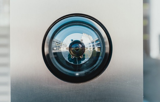
Charge Coupled Device (CCD) and Complementary Metal Oxide Semiconductor (CMOS) both have image sensors that are used for capturing digital images, but it is the technologies that are different. They each have their own set of strengths and weaknesses that give way to various applications. It is not as if one is superior to the other, but when you speak to vendors who only specialize in one of the forms of technology they will tell you that they feel otherwise. Throughout the last five years, there have been a lot of changes that have happened from both forms of technology. There are a lot of projections in regards to the demise of the technologies that have been proven false time and time again. Both forms of technology have a bright future, but there is still a need for the framework to be enhanced in regards to both of the CCD and CMOS imagers for their strengths and opportunities that they are going to be able to offer.

Light is converted into an electric charge that can be processed into an electronic signal through both of the imagers. Within a CCD sensor, each and every pixel’s charge has to be transferred through an extremely limited amount of output nodes, which at many times is only one. It is then converted into voltage, buffered, and sent as an analog signal from off the chip. This allows all of the pixels to be devoted to capturing light, while the output’s uniformity, which is crucial to the quality of your images, is high. On the other hand, a CMOS sensor is designed where each and every pixel has its own conversion from charge-to-voltage. The sensor will often include the use of amplifiers, noise correction and circuits that are digitized, which allow the chips to output bits of digital information. This allows the design complexity to be increased, while the area for light capturing is reduced. Uniformity is lowered because each pixel is actually doing its own conversion, but the chip could be built to need a smaller amount of off-chip circuitry for its basic operations.

Left: CCD ---Right: CMOS
During the late 1960s and early 1970s both of the CCD and CMOS imagers were invented. It was DALSA founder Dr. Chamberlain, who was also the CEO, which developed both of the technologies. CCD originally became the more dominant of the two technologies. It was due largely in part to the fact that it gave more exceptional imaging with the technology that was available. The imaging sensors used in the CMOS technology ended up requiring more uniformity and had smaller features beyond what the silicon water foundries were able to deliver at that time. It wasn’t until the 1990s that lithography was developed so designers could begin making their case for the CMOS imagers once again. There was now a renewed interest in CMOS that was based on the expectations of lower price consumptions, a camera-on-a-chip integration, and lower costs for fabrication due to the reusing of mainstream logic and fabricating for memory devices. Even though these benefits are only possible in theory, it will take a lot more time and money to be able to put them into practice at the same time as they are delivering a higher image quality. There is also going to be an additional process for adapting these changes into effect for the original projections.
When the imagers are designed properly you are going to get exceptional imaging performance from both the CCD and the CMOS imagers. In the photographic, scientific, and industrial applications CCD has provided the benchmarks for the performance in the highest image qualities while at the expense of the quality of images, which is also measured in quantum efficiency and noise. If you look at the CMOS imagers, you are going to find more integration, a lower dissipation of power and a smaller system size possibly. However, they often have tradeoffs that are required between the quality of the image and the cost of the device. There is really no clear line between the different types of applications that each one can serve. The designers of the CMOS technology have devoted a lot of their time and efforts into achieving high quality images, but the CCD designers ended up lowering their pixel sizes and the power requirements for their power. You are going to find a low-cost and low-power cell phone camera in the CCD technology, while the sensors in the CMOS technology are going to offer high-performance cameras for professional and industrial use, which directly contradicts all of the earlier stereotypes. The producers that have succeeded in producing the crossovers have years of experience rooted deeply in both of the technologies.
 At the chip level the costs are very similar for both the CCD and the CMOS. Early on the proponents of CMOS were claiming that the CMOS imagers were going to be a lot cheaper. They were supposed to be able to produce the same type of high-volume wafer processing lines as the mainstream login or the memory chips, but this has not been the case. The CMOS designers had to develop specialized, optimized, and lower-volume processors that are mixed-signal fabrications in order to accommodate the requirements for good imaging. It was very similar to that of the CCD designs. It has become a very slow and expensive process to be able to provide the processes at a successful lithography node that is smaller. There is an advantage to those who have a captive foundry because they are able to maintain the attention needed by the process engineers.
There are fewer components and less power that is required to operate the CMOS cameras, however, they are still going to need companion chips in order to have the optimal image quality. This process results in a higher cost and helps to reduce the advantages that are gained from lower power consumption. The CMOS devices are a lot more complex than the CCD devices, so they are going to cost a lot more to design them. The fabrication processes of the CCD tend to be a lot more mature and optimized. As a result, it is going to cost less to fabricate and design a CCD over a CMOS imager, in regards to a high-performance application. One of the most dominating influences of the device cost is the wafer size. The larger the wafer size is, the more devices it is going to be able to produce, which means the cost per device is going to be significantly reduced. The majority of the CMOS foundries are going to offer a 200mm device, whereas, the CCD foundries tend to offer a 150mm device. The majority of the captive foundries are going to use 150mm, 200mm, and 300mm for the production for the CCD and the CMOS devices.
 Beyond the pricing issue, you also have to worry about the sustainability potential. CMOS was priced below their actual costs in order to win business because they were trying to pursue a high volume and commodity applications from a limited base of various businesses. For some of those businesses, the risk that they took ended up paying off and the volume that was produced was enough to maintain a margin for viability. There were some businesses that ended up having to increase their costs, but others ended up going out of business completely. Some of the venture capitalists find high-risk startups to be interesting, whereas, imager customers are going to require a long-term support and stability plan.
There have been problems with the arrival and development of the on-chip integration, but speed is one of the areas where the CMOS imagers are able to demonstrate a considerable amount of strength. Cost advantages have been difficult for everyone to realize, but they do have a relative ease of use in the output structures that are parallel. In terms of industrial applications they are going to have great potential.
The CCD and CMOS imagers are going to remain complementary to each other. It is not so much a matter of the technology, but rather the choice is going to depend on the vendor and the application that they choose to use. There is one company that is going to remain technology neutral when it comes to the two options available to them. Teledyne DALSA’s is one of the few vendors that are able to offer real solutions with both of the CCDs and the CMOS technologies.
Even though there are a lot of differences between the two imagers, it is always going to remain in the hands of the vendor to decide which product they want to offer consumers. Everyone is going to have a different opinion of which imager is going to be the best one for them, but there is really no clear and definitive answer as to what the best option is. Take the time to go through what each one has to offer and try to make the most informed decision that you can, based on what exactly it is that you are looking for.